New Tools & IP Accelerate Development of 5nm Arm ‘Hercules’ SoCs
by Anton Shilov on October 10, 2019 3:30 PM EST- Posted in
- Semiconductors
- Samsung
- Arm
- Samsung Foundry
- 5nm
- 5LPE
- Hercules
- Synopsys

Arm, Synopsys, and Samsung Foundry have developed a set of optimized tools and IP that will enable chip designers to build next-generation SoCs based on Arm’s Hercules processor cores on Samsung’s 5LPE (5 nm, Low Power Early) node faster. The three companies expect the tools and IP to be used by designers of SoCs for a wide variety of applications.
The set of Synopsys tools are certified by Samsung Foundry for its 5LPE manufacturing technology, and now includes the Fusion Design Platform as well as QuickStart Implementation Kit that are enabled to optimize power, performance, and area for 5LPE designs. Meanwhile, Arm will provide Artisan Physical IP and POP IP tailored for Samsung’s 5LPE process. The IP packages will enable Arm’s partners to quickly develop 5LPE-optimized SoCs based on the Arm Hercules general-purpose CPU cores.
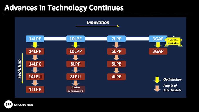
Samsung Foundry’s 5LPE fabrication process is the company’s 3rd Generation refinement of its 7LPP node that uses more EUV layers and features other improvements. The new technology provides an up to 25% higher ‘logic efficiency’, it also allows chip designers to lower power consumption of their SoCs by 20% (at the same performance and complexity) or improve their performance by 10% (at the same power and complexity). While developers can reuse 7LPP IP on SoCs build for 5LPE while taking advantage of the benefits the latter provides, to extract the maximum value of the new technology, optimized tools and IP are needed.
Considering that Arm’s Hercules are the company’s next-generation advanced CPU cores and 5LPE is a leading-edge process technology, Samsung expects the new tools and IP to be used for SoCs aimed at HPC, automotive, 5G, and AI applications.
Samsung expected to tape out the first 5LPE chips in the second half of 2019 and plans to start volume production using the node in the first half of 2020.
An official statement of Jaehong Park, executive vice president of Foundry Design Platform Development at Samsung Electronics, reads as follows.
"Synopsys' Fusion Design Platform and QuickStart Implementation Kits provide a design-ready solution for next-generation Arm-based processors. This is a great example of how Samsung 5LPE technology can be utilized to give designers a competitive advantage in their high-performance CPU designs. Through our close partnership with Arm and Synopsys, customers will now be able to extract maximum value out of our 5-nanometer processes for design applications targeted at high-performance and low-power markets."
Related Reading
- Samsung’s 5nm EUV Technology Gets Closer: Tools by Cadence & Synopsys Certified
- Samsung’s Aggressive EUV Plans: 6nm Production in H2, 5nm & 4nm On Track
- Synopsys to Accelerate Samsung’s 7nm Ramp with Yield Explorer Platform
- TSMC’s 5nm EUV Making Progress: PDK, DRM, EDA Tools, 3rd Party IP Ready
Source: Synopsys


8 Comments
View All Comments
isofilm - Thursday, October 10, 2019 - link
Poor Samsung, falling further and further behind TSMC, and with half the yield of TSMC, can only peel away TSMC clients with huge government subsidized discounts, only to have those clients running back to TSMC, once they realize they have been duped.lejeczek - Thursday, October 10, 2019 - link
And who is that beneficiary of those gov subsidies? And how to get those? I'd want some too.gdansk - Thursday, October 10, 2019 - link
Samsung Semi $4.3 billion in profit in 2019Q2 despite "low" DRAM prices. Not as glamorous or fast as TSMC but something the industry needs.brakdoo - Friday, October 11, 2019 - link
Making most of my money with asian tech stocks i have to say a few things:1. Samsung does not list net profits for subsidiaries. They list operating profits so it's not exactly what most people know as profits.
2. Samsung Semi had 3.4 trillion Kw ( < 3.1 bn USD) operating profit in q2 19.
3. All of Samsung Semi REVENUE minus memory was < 3.5 bn USD. That's Samsung LSI and fabs.
4. If you look at profit and revenue numbers of the past few quarters and multiply with the bit growth and ASP numbers they give during each earnings conference call you will see that Semi minus memory adds very little to their operating profit. Despite the DRAM price drops, memory remains their primary source of income.
Samsung Fabs are tiny compared to TSMC and they make much less revenue. They also spend much less CapEx. One has to question whether they had any profits at all. It is unclear how much they spend on R&D as no press release on this topic lists details to differentiate between Samsung LSI and fabs.
Samsungs fabs have to be seen as a strategic investment, not as source of income.
eastcoast_pete - Friday, October 11, 2019 - link
Good points! I agree that Samsung's fabs are more of a strategic investment than a profit center. Wouldn't be surprised if this Chaebol is also supported by the SK government to prevent the large tech sector there from being overly dependent on supplies from Taiwan, which might get cut off if China becomes more aggressive.Adonisds - Thursday, October 10, 2019 - link
What’s our current long term horizon of up to what point chip scaling will reach?brucethemoose - Thursday, October 10, 2019 - link
Many are predicting a "slow" death. So its not like we'll hit 3nm like a wall and the foundries will suddenly say "thats it, no more shrinks." Instead, shrinks will just get more incremental, more expensive, and increasingly augmented by other advances, but they'll probably keep trickling out for awhile.vladx - Sunday, October 13, 2019 - link
In the end the solution is still different materials that can provide better performance